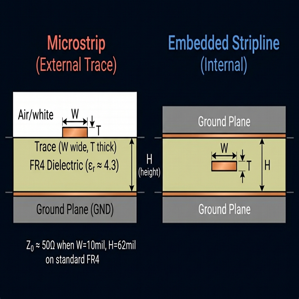
Left: Microstrip (outer layer) · Right: Embedded Stripline (inner layer)
Microstrip (External Trace)
A trace on the outer layer of a PCB above a ground plane. Uses IPC-2141A Hammerstad-Jensen formulas.
1 oz Cu ≈ 1.4 mil, 2 oz Cu ≈ 2.8 mil
Standard 1.6mm FR4 board ≈ 62 mil
FR4 ≈ 4.2–4.5 @ 1 GHz
Characteristic Impedance
—
Ω
Effective εr—
Propagation Delay—
Advertisement (In-Article)
What is Microstrip Impedance?
Characteristic impedance (Z0) is the impedance a transmission line presents to a signal at high frequencies. For reliable signal integrity in RF or high-speed digital PCB design, traces must be designed to match a target impedance — typically 50 Ω for RF and 50–100 Ω for differential pairs (e.g., USB, Ethernet, DDR). A mismatch causes reflections that degrade signal quality.
This calculator uses the IPC-2141A Hammerstad-Jensen formulas, which are the industry-standard approximations used by most PCB manufacturers and EDA tools.
Common Target Impedances
- 50 Ω — RF, SMA connectors, Wi-Fi/Bluetooth antennas
- 75 Ω — Video (CVBS, SDI)
- 90 Ω differential — USB 2.0
- 100 Ω differential — USB 3.x, Ethernet, DDR data lines