Understanding High-Side MOSFET Switching
What is a High-Side Switch?
A high-side switch is placed between the positive power supply (Vcc) and the load. When the switch is open, the load is completely disconnected from the power source and is safely sitting at ground potential (0V). This is often preferred for safety and isolation reasons, particularly in automotive and industrial applications where loads sharing a common chassis ground must be completely de-energized when turned off.
Using a P-Channel MOSFET
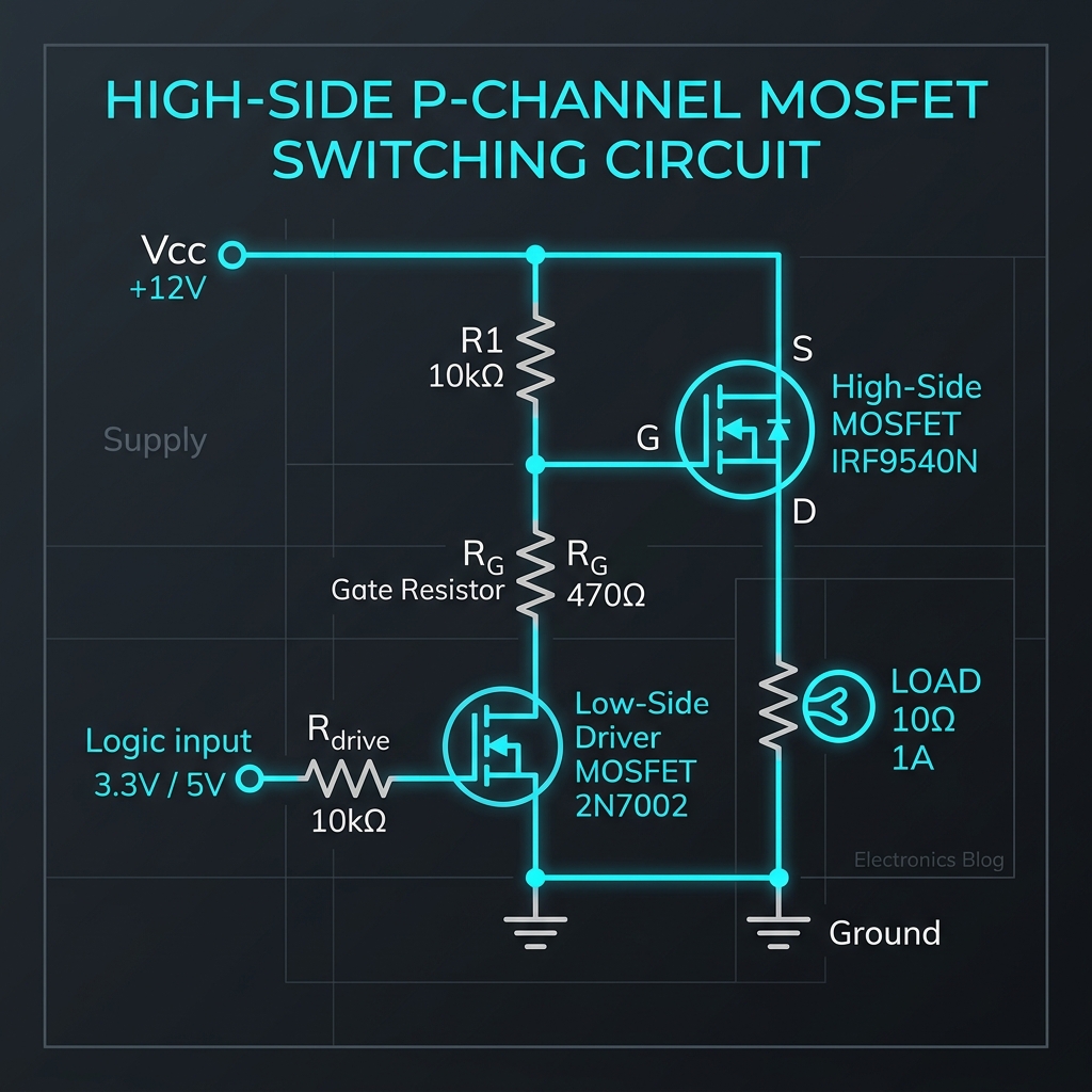
For high-side switching, a P-Channel MOSFET is typically the easiest component to use. Its Source is tied to Vcc, and the Drain is connected to the load. To turn the MOSFET ON, the Gate voltage must be pulled lower than the Source voltage (Vgs < 0). To turn it OFF, the Gate is pulled up to Vcc (Vgs = 0).
Because microcontrollers operate at lower voltages (like 3.3V or 5V) compared to many loads (12V or 24V), directly driving a P-Channel MOSFET gate from a microcontroller pin can be impossible or dangerous. Therefore, a small N-channel MOSFET or NPN transistor is usually employed as a "level shifter" or gate driver to pull the P-channel gate down to ground.
Pros and Cons
- Pro: Safer during faults. A short-to-ground fault on the load wiring will just blow a fuse, rather than turning the load permanently on.
- Pro: Load sits at 0V when off, reducing corrosion and preventing unexpected ground loops.
- Con: P-Channel MOSFETs generally have higher RDS(on) and cost more than N-Channel equivalents of the same size.
- Con: Driving them from low-voltage logic requires extra level-shifting components.