Introduction to openEMS
Introduction to openEMS
openEMS is a free and open-source 3D electromagnetic (EM) field solver. It utilizes the Finite-Difference Time-Domain (FDTD) method to simulate Maxwell's equations. For PCB designers and engineers working on high-speed digital or RF circuits, it serves as an accessible alternative to expensive commercial tools like Ansys HFSS, Keysight ADS, or Simbeor.1. Core Capabilities
openEMS is highly capable of performing the rigorous analysis required for modern hardware design:
* S-Parameter Extraction: Calculates S-parameters (Insertion loss, return loss, crosstalk) for traces, vias, and connectors.
* Impedance Calculation: Determines the characteristic impedance ($Z_0$) of complex trace geometries, differential pairs, and coplanar waveguides.
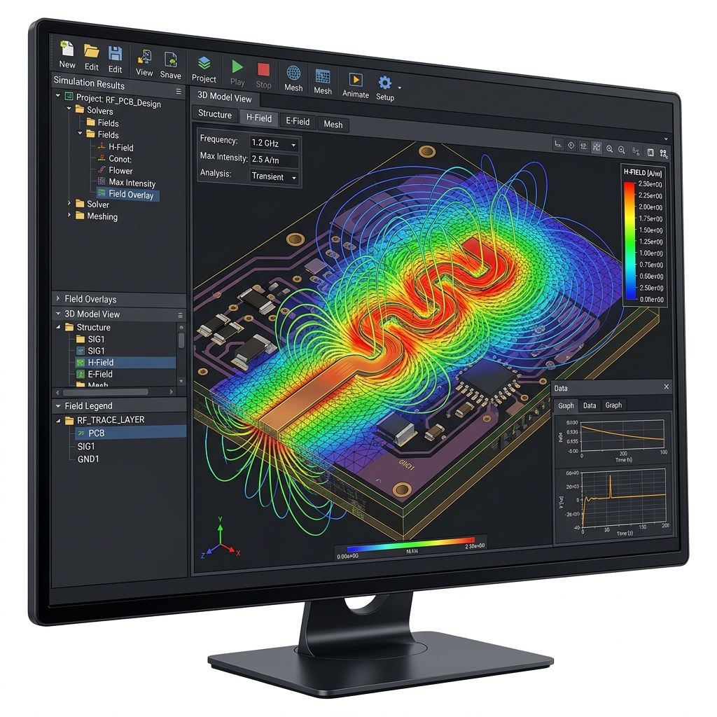
* Near-Field and Far-Field Visualization: Simulates and visualizes how electromagnetic fields propagate, which is critical for identifying EMI (Electromagnetic Interference) issues and analyzing antenna radiation patterns.
* Time-Domain Reflectometry (TDR): Simulates TDR to locate impedance discontinuities along a signal path.
2. How it Works (The Workflow)
Unlike commercial EM solvers, openEMS does not have a standalone Graphical User Interface (GUI). Instead, it relies on a scripting interface.
- Scripting Environment: You define your simulation geometry, material properties, mesh size, and excitation ports using scripts. The primary supported languages are Python, MATLAB, and GNU Octave.
- AppCSXCAD (Visualization): openEMS comes with a companion viewer called AppCSXCAD. Before running the heavy simulation, you use this viewer to visually verify that your geometry, mesh, and ports have been scripted correctly.
- Simulation Engine: Once verified, the script calls the openEMS C++ engine to perform the FDTD simulation. This step can be computationally intensive and scales well with multi-core CPUs.
- Post-Processing: The output data (like voltage and current over time) is pulled back into your Python/MATLAB script, where you can apply Fast Fourier Transforms (FFT) to convert it into frequency-domain data (like S-parameters) and plot the results.
3. PCB Workflow and Integration
Simulating an entire complex PCB (like an FPGA board) in a 3D EM solver is extremely difficult and computationally expensive. The best practice is to isolate critical sections (like a single high-speed memory trace or a differential pair).
To bridge the gap between EDA tools (like Altium Designer) and openEMS, the community has developed helper tools:
* gerber2ems: An open-source tool developed by Antmicro. It automates the conversion of standard PCB manufacturing files (Gerbers) into the geometric formats required by openEMS. This prevents the engineer from having to manually script the exact coordinates of every copper trace.
* Workflow:
1. Export Gerbers from Altium for the specific layers/traces you want to analyze.
2. Use gerber2ems to translate the geometry.
3. Use a Python script to define the mesh, attach ports to the ends of the traces, and run the openEMS simulation.
4. Pros and Cons
Pros:* Cost: 100% Free and open-source.
* Transparency: Full control over the simulation parameters and mesh.
* Automation: Because it is script-driven, it is highly suitable for automated parameter sweeps and optimization loops.
Cons:* Steep Learning Curve: Requires programming knowledge (Python/MATLAB) and a strong understanding of EM simulation principles (like how to define a proper FDTD mesh and absorbing boundary conditions).
* No Native PCB Importer: Lacks the seamless "import board and click simulate" experience of commercial SI/PI tools.
*For more information, documentation, and tutorials, visit the official openEMS project page: [https://openems.de](https://openems.de)*